1. Crystal Framework and Polytypism of Silicon Carbide
1.1 Cubic and Hexagonal Polytypes: From 3C to 6H and Past
(Silicon Carbide Ceramics)
Silicon carbide (SiC) is a covalently adhered ceramic made up of silicon and carbon atoms arranged in a tetrahedral sychronisation, creating among the most complex systems of polytypism in products scientific research.
Unlike most porcelains with a single secure crystal structure, SiC exists in over 250 well-known polytypes– unique piling sequences of close-packed Si-C bilayers along the c-axis– varying from cubic 3C-SiC (additionally called β-SiC) to hexagonal 6H-SiC and rhombohedral 15R-SiC.
The most usual polytypes utilized in design applications are 3C (cubic), 4H, and 6H (both hexagonal), each displaying somewhat different electronic band structures and thermal conductivities.
3C-SiC, with its zinc blende framework, has the narrowest bandgap (~ 2.3 eV) and is commonly expanded on silicon substratums for semiconductor tools, while 4H-SiC supplies superior electron movement and is favored for high-power electronic devices.
The solid covalent bonding and directional nature of the Si– C bond confer extraordinary solidity, thermal security, and resistance to slip and chemical strike, making SiC suitable for severe setting applications.
1.2 Issues, Doping, and Digital Quality
Despite its structural complexity, SiC can be doped to achieve both n-type and p-type conductivity, enabling its usage in semiconductor tools.
Nitrogen and phosphorus work as contributor impurities, presenting electrons right into the transmission band, while aluminum and boron serve as acceptors, producing holes in the valence band.
Nevertheless, p-type doping performance is restricted by high activation energies, particularly in 4H-SiC, which positions obstacles for bipolar device design.
Native defects such as screw misplacements, micropipes, and stacking faults can degrade device efficiency by functioning as recombination facilities or leak paths, demanding premium single-crystal growth for digital applications.
The broad bandgap (2.3– 3.3 eV depending on polytype), high breakdown electrical area (~ 3 MV/cm), and outstanding thermal conductivity (~ 3– 4 W/m · K for 4H-SiC) make SiC far superior to silicon in high-temperature, high-voltage, and high-frequency power electronic devices.
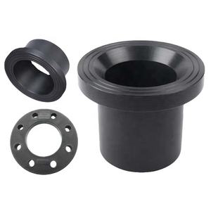
2. Processing and Microstructural Engineering
( Silicon Carbide Ceramics)
2.1 Sintering and Densification Strategies
Silicon carbide is naturally difficult to densify because of its solid covalent bonding and low self-diffusion coefficients, needing advanced handling methods to accomplish complete density without additives or with very little sintering aids.
Pressureless sintering of submicron SiC powders is feasible with the addition of boron and carbon, which promote densification by eliminating oxide layers and improving solid-state diffusion.
Hot pushing applies uniaxial stress throughout home heating, making it possible for complete densification at lower temperature levels (~ 1800– 2000 ° C )and creating fine-grained, high-strength components appropriate for reducing tools and wear parts.
For huge or complex forms, response bonding is used, where permeable carbon preforms are infiltrated with molten silicon at ~ 1600 ° C, creating β-SiC in situ with minimal contraction.
Nonetheless, recurring complimentary silicon (~ 5– 10%) stays in the microstructure, limiting high-temperature performance and oxidation resistance above 1300 ° C.
2.2 Additive Manufacturing and Near-Net-Shape Construction
Current breakthroughs in additive production (AM), particularly binder jetting and stereolithography making use of SiC powders or preceramic polymers, make it possible for the manufacture of intricate geometries formerly unattainable with traditional approaches.
In polymer-derived ceramic (PDC) paths, liquid SiC forerunners are shaped by means of 3D printing and after that pyrolyzed at high temperatures to generate amorphous or nanocrystalline SiC, usually requiring further densification.
These methods decrease machining costs and product waste, making SiC extra accessible for aerospace, nuclear, and warmth exchanger applications where detailed layouts boost performance.
Post-processing steps such as chemical vapor seepage (CVI) or liquid silicon seepage (LSI) are occasionally used to boost thickness and mechanical honesty.
3. Mechanical, Thermal, and Environmental Efficiency
3.1 Stamina, Firmness, and Wear Resistance
Silicon carbide ranks among the hardest recognized products, with a Mohs hardness of ~ 9.5 and Vickers firmness exceeding 25 Grade point average, making it very resistant to abrasion, disintegration, and scraping.
Its flexural stamina normally ranges from 300 to 600 MPa, depending on processing technique and grain dimension, and it maintains stamina at temperature levels as much as 1400 ° C in inert ambiences.
Crack sturdiness, while modest (~ 3– 4 MPa · m ¹/ ²), is sufficient for numerous architectural applications, particularly when integrated with fiber support in ceramic matrix compounds (CMCs).
SiC-based CMCs are used in generator blades, combustor liners, and brake systems, where they supply weight financial savings, fuel performance, and expanded service life over metallic counterparts.
Its superb wear resistance makes SiC perfect for seals, bearings, pump elements, and ballistic armor, where toughness under severe mechanical loading is crucial.
3.2 Thermal Conductivity and Oxidation Security
One of SiC’s most beneficial residential properties is its high thermal conductivity– as much as 490 W/m · K for single-crystal 4H-SiC and ~ 30– 120 W/m · K for polycrystalline forms– exceeding that of many metals and enabling effective heat dissipation.
This building is important in power electronics, where SiC tools create much less waste heat and can run at higher power thickness than silicon-based tools.
At elevated temperature levels in oxidizing environments, SiC forms a safety silica (SiO TWO) layer that reduces further oxidation, giving good ecological durability approximately ~ 1600 ° C.
Nonetheless, in water vapor-rich atmospheres, this layer can volatilize as Si(OH)FOUR, resulting in increased destruction– a vital difficulty in gas turbine applications.
4. Advanced Applications in Power, Electronics, and Aerospace
4.1 Power Electronics and Semiconductor Devices
Silicon carbide has revolutionized power electronics by enabling tools such as Schottky diodes, MOSFETs, and JFETs that operate at greater voltages, regularities, and temperature levels than silicon equivalents.
These tools lower power losses in electric vehicles, renewable resource inverters, and industrial electric motor drives, contributing to international power effectiveness improvements.
The ability to run at junction temperature levels above 200 ° C permits streamlined air conditioning systems and raised system integrity.
Moreover, SiC wafers are utilized as substratums for gallium nitride (GaN) epitaxy in high-electron-mobility transistors (HEMTs), incorporating the benefits of both wide-bandgap semiconductors.
4.2 Nuclear, Aerospace, and Optical Equipments
In atomic power plants, SiC is a key element of accident-tolerant fuel cladding, where its reduced neutron absorption cross-section, radiation resistance, and high-temperature toughness enhance safety and security and efficiency.
In aerospace, SiC fiber-reinforced compounds are utilized in jet engines and hypersonic vehicles for their lightweight and thermal stability.
In addition, ultra-smooth SiC mirrors are utilized in space telescopes as a result of their high stiffness-to-density proportion, thermal security, and polishability to sub-nanometer roughness.
In recap, silicon carbide porcelains represent a cornerstone of modern sophisticated products, combining exceptional mechanical, thermal, and electronic homes.
Via accurate control of polytype, microstructure, and processing, SiC continues to make it possible for technical breakthroughs in power, transport, and extreme environment engineering.
5. Distributor
TRUNNANO is a supplier of Spherical Tungsten Powder with over 12 years of experience in nano-building energy conservation and nanotechnology development. It accepts payment via Credit Card, T/T, West Union and Paypal. Trunnano will ship the goods to customers overseas through FedEx, DHL, by air, or by sea. If you want to know more about Spherical Tungsten Powder, please feel free to contact us and send an inquiry(sales5@nanotrun.com).
Tags: silicon carbide ceramic,silicon carbide ceramic products, industry ceramic
All articles and pictures are from the Internet. If there are any copyright issues, please contact us in time to delete.
Inquiry us

