1. Essential Features and Nanoscale Actions of Silicon at the Submicron Frontier
1.1 Quantum Confinement and Electronic Structure Change
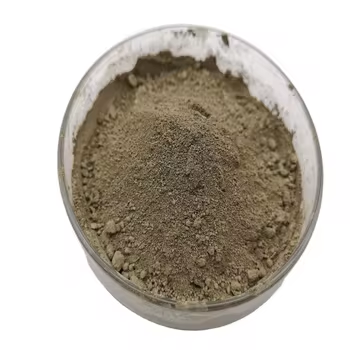
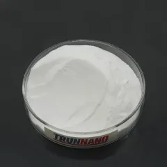
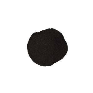
(Nano-Silicon Powder)
Nano-silicon powder, made up of silicon fragments with particular dimensions listed below 100 nanometers, stands for a standard change from bulk silicon in both physical behavior and functional energy.
While mass silicon is an indirect bandgap semiconductor with a bandgap of approximately 1.12 eV, nano-sizing generates quantum arrest results that basically change its electronic and optical residential properties.
When the particle size strategies or falls below the exciton Bohr distance of silicon (~ 5 nm), fee carriers become spatially constrained, bring about a widening of the bandgap and the introduction of noticeable photoluminescence– a phenomenon missing in macroscopic silicon.
This size-dependent tunability enables nano-silicon to emit light across the noticeable spectrum, making it an encouraging prospect for silicon-based optoelectronics, where conventional silicon fails due to its inadequate radiative recombination performance.
In addition, the increased surface-to-volume ratio at the nanoscale boosts surface-related phenomena, including chemical reactivity, catalytic activity, and communication with electromagnetic fields.
These quantum impacts are not merely scholastic curiosities yet create the foundation for next-generation applications in power, noticing, and biomedicine.
1.2 Morphological Diversity and Surface Chemistry
Nano-silicon powder can be manufactured in various morphologies, consisting of spherical nanoparticles, nanowires, permeable nanostructures, and crystalline quantum dots, each offering distinctive advantages depending upon the target application.
Crystalline nano-silicon usually preserves the diamond cubic structure of mass silicon however exhibits a greater density of surface area defects and dangling bonds, which have to be passivated to support the product.
Surface area functionalization– frequently accomplished via oxidation, hydrosilylation, or ligand attachment– plays a vital duty in figuring out colloidal security, dispersibility, and compatibility with matrices in composites or biological environments.
As an example, hydrogen-terminated nano-silicon reveals high reactivity and is vulnerable to oxidation in air, whereas alkyl- or polyethylene glycol (PEG)-layered bits show boosted security and biocompatibility for biomedical use.
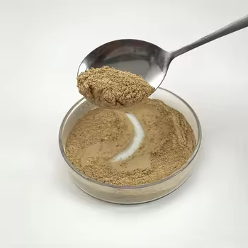
( Nano-Silicon Powder)
The existence of a native oxide layer (SiOₓ) on the bit surface area, even in marginal amounts, substantially affects electrical conductivity, lithium-ion diffusion kinetics, and interfacial responses, especially in battery applications.
Understanding and regulating surface area chemistry is for that reason essential for utilizing the complete capacity of nano-silicon in useful systems.
2. Synthesis Techniques and Scalable Construction Techniques
2.1 Top-Down Approaches: Milling, Etching, and Laser Ablation
The production of nano-silicon powder can be generally classified right into top-down and bottom-up methods, each with unique scalability, pureness, and morphological control features.
Top-down methods include the physical or chemical decrease of mass silicon into nanoscale pieces.
High-energy sphere milling is a commonly used industrial method, where silicon chunks are subjected to extreme mechanical grinding in inert atmospheres, causing micron- to nano-sized powders.
While cost-effective and scalable, this method often presents crystal issues, contamination from milling media, and broad particle size distributions, needing post-processing purification.
Magnesiothermic reduction of silica (SiO ₂) complied with by acid leaching is an additional scalable path, especially when utilizing natural or waste-derived silica resources such as rice husks or diatoms, offering a lasting path to nano-silicon.
Laser ablation and reactive plasma etching are a lot more accurate top-down approaches, capable of generating high-purity nano-silicon with regulated crystallinity, though at higher expense and reduced throughput.
2.2 Bottom-Up Methods: Gas-Phase and Solution-Phase Growth
Bottom-up synthesis permits higher control over fragment size, form, and crystallinity by building nanostructures atom by atom.
Chemical vapor deposition (CVD) and plasma-enhanced CVD (PECVD) enable the growth of nano-silicon from gaseous forerunners such as silane (SiH FOUR) or disilane (Si ₂ H ₆), with parameters like temperature level, pressure, and gas flow dictating nucleation and development kinetics.
These approaches are specifically efficient for producing silicon nanocrystals installed in dielectric matrices for optoelectronic devices.
Solution-phase synthesis, including colloidal routes making use of organosilicon compounds, enables the production of monodisperse silicon quantum dots with tunable discharge wavelengths.
Thermal decay of silane in high-boiling solvents or supercritical fluid synthesis likewise generates high-quality nano-silicon with slim dimension distributions, ideal for biomedical labeling and imaging.
While bottom-up approaches normally generate premium material high quality, they face obstacles in large production and cost-efficiency, necessitating ongoing research study into crossbreed and continuous-flow procedures.
3. Power Applications: Transforming Lithium-Ion and Beyond-Lithium Batteries
3.1 Role in High-Capacity Anodes for Lithium-Ion Batteries
Among the most transformative applications of nano-silicon powder lies in power storage, especially as an anode product in lithium-ion batteries (LIBs).
Silicon uses an academic certain capacity of ~ 3579 mAh/g based upon the development of Li ₁₅ Si Four, which is nearly ten times more than that of standard graphite (372 mAh/g).
However, the huge volume growth (~ 300%) during lithiation causes fragment pulverization, loss of electric contact, and continuous solid electrolyte interphase (SEI) formation, leading to fast capability discolor.
Nanostructuring reduces these issues by shortening lithium diffusion paths, accommodating stress more effectively, and minimizing fracture possibility.
Nano-silicon in the kind of nanoparticles, permeable frameworks, or yolk-shell structures allows relatively easy to fix cycling with enhanced Coulombic efficiency and cycle life.
Business battery technologies now incorporate nano-silicon blends (e.g., silicon-carbon composites) in anodes to improve power density in customer electronics, electric automobiles, and grid storage space systems.
3.2 Prospective in Sodium-Ion, Potassium-Ion, and Solid-State Batteries
Past lithium-ion systems, nano-silicon is being discovered in arising battery chemistries.
While silicon is much less responsive with salt than lithium, nano-sizing enhances kinetics and makes it possible for restricted Na ⁺ insertion, making it a prospect for sodium-ion battery anodes, particularly when alloyed or composited with tin or antimony.
In solid-state batteries, where mechanical stability at electrode-electrolyte user interfaces is vital, nano-silicon’s ability to go through plastic contortion at tiny scales lowers interfacial stress and improves call maintenance.
In addition, its compatibility with sulfide- and oxide-based strong electrolytes opens up methods for much safer, higher-energy-density storage space services.
Research continues to optimize user interface design and prelithiation techniques to make the most of the long life and performance of nano-silicon-based electrodes.
4. Arising Frontiers in Photonics, Biomedicine, and Composite Materials
4.1 Applications in Optoelectronics and Quantum Light
The photoluminescent residential properties of nano-silicon have revitalized efforts to create silicon-based light-emitting tools, a long-lasting difficulty in integrated photonics.
Unlike bulk silicon, nano-silicon quantum dots can show effective, tunable photoluminescence in the noticeable to near-infrared range, enabling on-chip source of lights suitable with corresponding metal-oxide-semiconductor (CMOS) innovation.
These nanomaterials are being incorporated into light-emitting diodes (LEDs), photodetectors, and waveguide-coupled emitters for optical interconnects and noticing applications.
In addition, surface-engineered nano-silicon shows single-photon discharge under specific flaw setups, positioning it as a potential platform for quantum data processing and secure interaction.
4.2 Biomedical and Environmental Applications
In biomedicine, nano-silicon powder is getting interest as a biocompatible, biodegradable, and safe alternative to heavy-metal-based quantum dots for bioimaging and medicine delivery.
Surface-functionalized nano-silicon particles can be developed to target particular cells, release healing representatives in feedback to pH or enzymes, and give real-time fluorescence monitoring.
Their degradation into silicic acid (Si(OH)FOUR), a naturally taking place and excretable substance, lessens lasting toxicity issues.
In addition, nano-silicon is being investigated for environmental removal, such as photocatalytic destruction of pollutants under noticeable light or as a lowering agent in water treatment procedures.
In composite materials, nano-silicon improves mechanical toughness, thermal security, and put on resistance when integrated right into metals, porcelains, or polymers, particularly in aerospace and automotive components.
In conclusion, nano-silicon powder stands at the crossway of essential nanoscience and commercial development.
Its distinct combination of quantum impacts, high reactivity, and adaptability across power, electronic devices, and life sciences emphasizes its role as a key enabler of next-generation modern technologies.
As synthesis strategies development and combination difficulties are overcome, nano-silicon will remain to drive development towards higher-performance, sustainable, and multifunctional material systems.
5. Vendor
TRUNNANO is a supplier of Spherical Tungsten Powder with over 12 years of experience in nano-building energy conservation and nanotechnology development. It accepts payment via Credit Card, T/T, West Union and Paypal. Trunnano will ship the goods to customers overseas through FedEx, DHL, by air, or by sea. If you want to know more about Spherical Tungsten Powder, please feel free to contact us and send an inquiry(sales5@nanotrun.com).
Tags: Nano-Silicon Powder, Silicon Powder, Silicon
All articles and pictures are from the Internet. If there are any copyright issues, please contact us in time to delete.
Inquiry us


